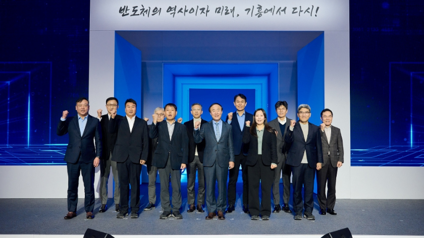
Samsung Electronics has inaugurated its new semiconductor research and development facility, NRD-K, in Korea.
The site, which spans 109,000 square metres, is located in Samsung’s Giheung campus, where the company developed the world’s first 64-megabit DRAM chip in the early 90s.
The new NRD-K facility will be used to explore new process technologies and manufacturing tools and will feature High NA extreme ultra-violet (EUV) lithography to accelerate next-generation memory semiconductors such as 3D DRAM and V-NAND with more than 1,000 layers.
“NRD-K will bolster our development speed, enabling the company to create a virtuous cycle to accelerate fundamental research on next-generation technology and mass production, said Young Hyun Jun, vice chair and head of the device solutions division at Samsung.
Samsung broke ground on the site in 2022, with the company planning to invest KRW 20 trillion (US$14.8 billion) in the site by 2030.
An R&D-dedicated line is scheduled to begin operation at the site in mid-2025.


